At the Huawei Shanghai launch: the future of chip design
Moore's Law has guided chip design for 50 years, and Huawei just proposed a way around it. Inside LogicFolding, and the roundtable that followed.
Moore's Law has guided chip design for over 50 years. Huawei just proposed a way around it, and it's shipping this autumn.
If you aren't trying to shrink transistor size, can you still increase chip performance?
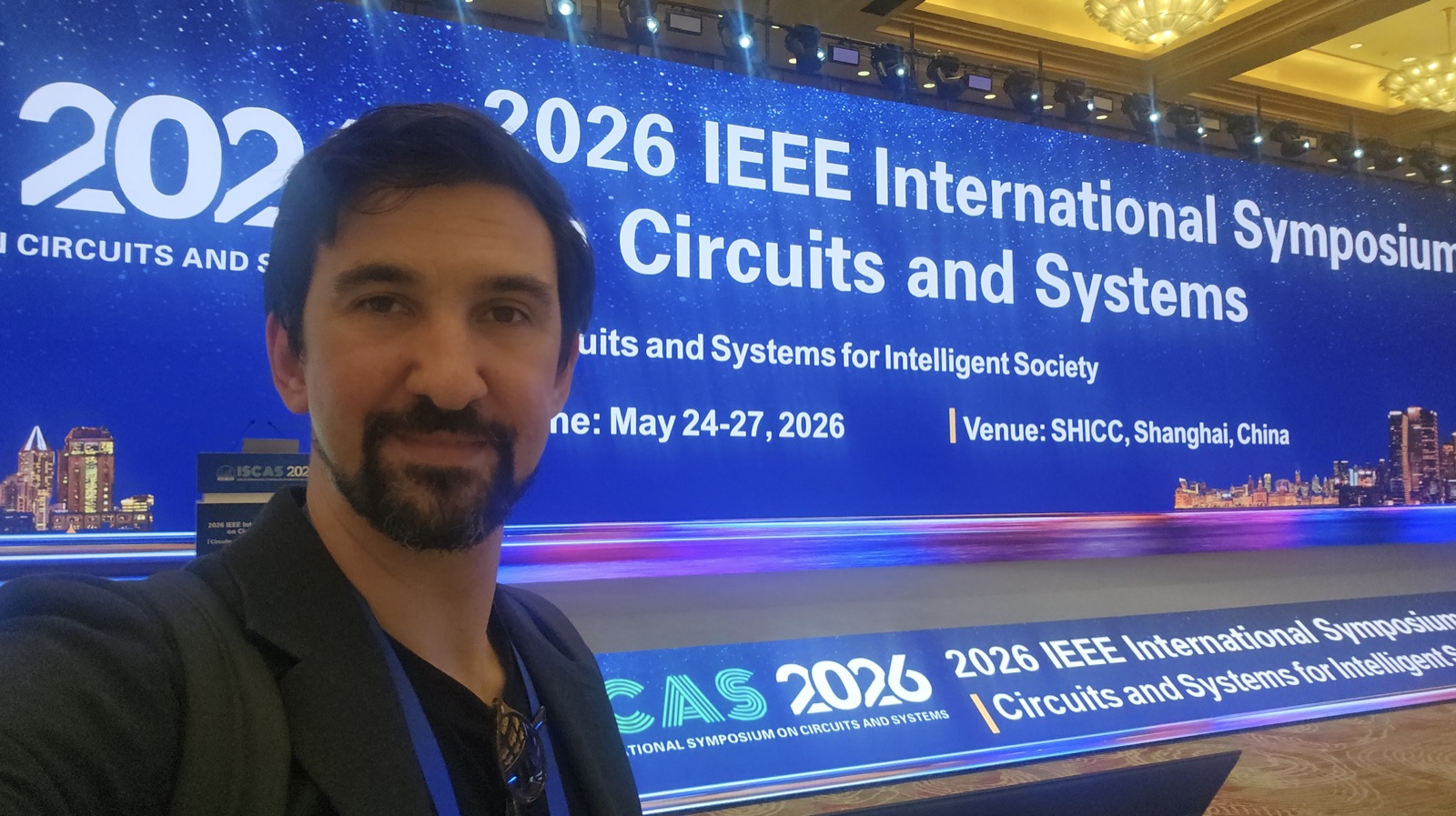
I was invited to IEEE ISCAS 2026 in Shanghai to hear He Tingbo, President of Huawei Semiconductor, unveil their work on LogicFolding, where rather than reduce transistor size, they optimise on τ-scaling by folding chip circuitry vertically. Creating skyscrapers instead of street grids, with denser logic and shorter signal paths.
This has a pretty dramatic effect. The first commercial silicon using LogicFolding, the Kirin 2026, ships this autumn with 53.5% higher transistor density and 41% better energy efficiency. And it's built on lithography the rest of the market had written off as only able to produce diminishing returns.
After the announcement, I joined He Tingbo and a private media roundtable. She talked through her design philosophy, and the question she's actually been operating against:
If you can't catch up on lithography, how do you make the question obsolete?
If LogicFolding scales, it's interesting to think about what the competitive frontier in semiconductors actually looks like in five years. Architecture, packaging, or something else?